Important changes to forums and questions
All forums and questions are now archived. To start a new conversation or read the latest updates go to forums.mbed.com.
7 years, 2 months ago.
Controlling AD9910 DDS with mbed
Hi,
I'm a student who wants to work with DDS AD9910 with SPI bus.
here you can find datasheet :http://www.analog.com/media/en/technical-documentation/data-sheets/AD9910.pdf
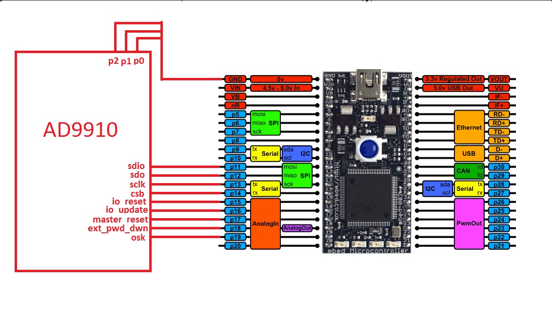
I using this configuration :

is that right ?
We want to have a frequency out of 100 Mhz, what kind of word we have to send ?
we want to sweep from 1MHz to 200 with a step of 5Hz.
I have a code but don't work !
can you help me ?
Thanks in advance for your help.
here is the code was adapted :
#include "mbed.h"
#include "AD9910.h"

Serial pc(USBTX, USBRX);

DigitalOut myled(LED1);
DigitalOut _fud(p16);

AD9910 myDevice(p11, p12, p13, p14, p15); //mosi, miso, sclk, cs, rst.

DigitalOut MASTER_RESET(p17);//DDS' Master_Reset pin.
DigitalOut EXT_PWD(p18);     //EXT_POWER_DOWN pin of DDS.


int main() {


EXT_PWD=1;
wait(0.1);
EXT_PWD=0;
wait(0.1);
MASTER_RESET=1;
wait(0.1);
MASTER_RESET=0;
wait(0.1);


    _fud.write(0);
        // in register 2:
//bit3-bit7 contain the multiplication value for the clock. multiply the 10 MHz input by 10: [01010], the vco is then not in the upper range, therefore bit2=0,
        // from this follows bit7-bit0: 00 00 0101 0000 -> 00 00 50
        myDevice.CFR2_write(000050);
        // now we have a 100 MHz clock, the frequency tuning word for around 6 MHz output is ((12.5:2)/100)*2^(32) =268435456
        //= 10000000
        myDevice.FTW0_write(0x10000000);
// issue I/O update
    _fud.write(1);
    wait(0.1);
    _fud.write(0);

        uint32_t c2;
        c2 = myDevice.CFR2_read();
        pc.printf("c2= %X\n", c2);

        uint32_t ftwo;
        ftwo = myDevice.FTWO_read();
        pc.printf("FTWO = %X\n", ftwo);
   return 0;
}


//#################### AD9910.h ###########################
#ifndef AD9910_H
#define AD9910_H
#include "mbed.h"
class AD9910 {
protected:
    SPI         _spi;
    DigitalOut  _cs;
    DigitalOut  _rst;

public:
    AD9910(PinName mosi, PinName miso, PinName sclk, PinName cs, PinName rst) :
        _spi(mosi, miso, sclk), _cs(cs), _rst(rst)
    {
        // see http://mbed.org/handbook/SPI and page 23 why format 0
        _spi.format(8, 0);
        _spi.frequency(1000000);
        // master reset the device:
        _rst.write(1);
         wait(0.1);
        _rst.write(0);
    };
    // Write a 32bit register at the specified address.
    void write_reg_4byte(uint32_t address, uint32_t value) {
      // Instruction byte: page 25 in datasheet, we want to write (0), so 0100 + internal adress of the register to be written in
        _spi.write(0x00 | (address & 0x1F));
        _spi.write((value >> 24) & 0xFF);
        _spi.write((value >> 16) & 0xFF);
        _spi.write((value >> 8) & 0xFF);
        _spi.write((value >> 0) & 0xFF);
    }

    // Write a 24bit register at the specified address.
    void write_reg_3byte(uint32_t address, uint32_t value) {
      // Instruction byte: page 25 in datasheet, we want to write (0), so 0100 + internal adress of the register to be written in
        _spi.write(0x00 | (address & 0x1F));
        _spi.write((value >> 16) & 0xFF);
        _spi.write((value >> 8) & 0xFF);
        _spi.write((value >> 0) & 0xFF);
    }

    // Read a 32bit register at the specified address.
    uint32_t read_reg_4byte(uint32_t address) {
        uint32_t value = 0x00000000;
        _spi.write(0x80 | (address & 0x1F)); // Instruction byte
        value |= _spi.write(0x00);
        value = value << 8;
        value |= _spi.write(0x00);
        value = value << 8;
        value |= _spi.write(0x00);
        value = value << 8;
        value |= _spi.write(0x00);
        return value;
    }

    uint32_t read_reg_3byte(uint32_t address) {
        uint32_t value = 0x000000;
        _spi.write(0x80 | (address & 0xF)); // Instruction byte
        value |= _spi.write(0x00);
        value = value << 8;
        value |= _spi.write(0x00);
        value = value << 8;
        value |= _spi.write(0x00);
        return value;
    }
    // Write
    void CFR1_write(uint32_t reg) { write_reg_4byte(0x00, reg); }
    void CFR2_write(uint32_t reg) { write_reg_3byte(0x01, reg); }
    void FTW0_write(uint32_t reg) { write_reg_4byte(0x04, reg); }

    // Read
    uint32_t CFR1_read(void) { return read_reg_4byte(0x0); }
    uint32_t CFR2_read(void) { return read_reg_3byte(0x1); }
    uint32_t FTWO_read(void) { return read_reg_4byte(0x4); }
};